Why Organic Photodetector (OPD) ?
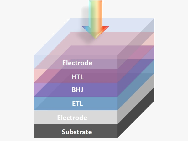
OPD is an emerging optical sensor which using organic semiconductor as photoactive layer, it is promising to replace state of art silicon and inorganic photodetectors with following advantages:
 Tunable Spectral Response
By adjusting the chemical structure of the organic semiconductor, the spectral sensitivity of OPD can be customized to various wavelengths.
- Short-wavelength and Near Infrared Sensing (SWIR and NIR)
Mainstream Silicon photodetector has no spectral response beyond 1000 nm while alternative inorganic photodetectors, such as III-V semiconductor are known for the high cost. In this regards, OPD could complement above existing photodetector technologies’ shortcoming by offering tunable spectrum response and cost-effective production, respectively.
- Excellent Absorption Coefficient
The absorption coefficient of organic semiconductor is 10~100 times higher than inorganic semiconductors, it keeps the sensitivity of photodetector under sub-micro pixel.
- Enhance Next-generation Image Sensor
Thanks to readiness of OLED on silicon product, the process compatibility of organic semiconductor on a readout integrated circuit (ROIC) is proven. Integration of an OPD with a ROIC offers several benefits, including a larger fill factor and thinner sensor structure, it enhances the sensitivity of organic image sensor to achieve the wide dynamic range image.
- Large-are Processibility
Solution processable OPD offers possibility of using spin or slot-ide coating to fabricate the device, compatible to large area process up to 12 inch wafer and Gen 8.5 TFT glass or plastic substrate with high throughput.
- Small CO2 Footprint and Environmental Friendly
OPD, being lead-free and contain no rare earth materials, can be fabricated by non-vacuum and low temperature process, using low energy consumption and produces less CO2 compares to that of the state of art semiconductor process.